 |
ToToTEK.COM
Help & Support Forum
|
| View previous topic :: View next topic |
| Author |
Message |
1541
Joined: 09 Apr 2008
Posts: 15
|
 Posted: Tue Apr 22, 2008 10:55 pm Post subject: Re: Super Wildcard SWC3201 RAM Upgrade Posted: Tue Apr 22, 2008 10:55 pm Post subject: Re: Super Wildcard SWC3201 RAM Upgrade |
 |
|
| rcade wrote: | | The files came from the Schweino archive (I think) and I had someone make several sets for me. They don't work without the board mods, though. |
What happens if the new programmable logic is installed without making the modifications? Can it cause hardware damage?
| rcade wrote: | | I have the mods for one board revision but not the other. |
Please post the information that you have.
|
|
| Back to top |
|
 |
1541
Joined: 09 Apr 2008
Posts: 15
|
| Posted: Fri Apr 25, 2008 8:10 pm Post subject: |
|
|
| The new EPROM with 2.8CC firmware and the two programmable logic chips have now been installed. Compatibility is better, three games that used to crash with 1.8C and the old programmable logic now work fine. Does your unit recognize 24 megabits of DRAM without the hardware modifications, rcade?
|
|
| Back to top |
|
|
rcade
Joined: 13 Mar 2008
Posts: 30
|
|
| Back to top |
|
|
1541
Joined: 09 Apr 2008
Posts: 15
|
| Posted: Thu May 08, 2008 6:14 am Post subject: Re: Super Wildcard SWC3201 RAM Upgrade |
|
|
| rcade wrote: | | Here are the two photos of the board with the Goldstar chip. Mine has a Motorola chip and the board layout is much different. |
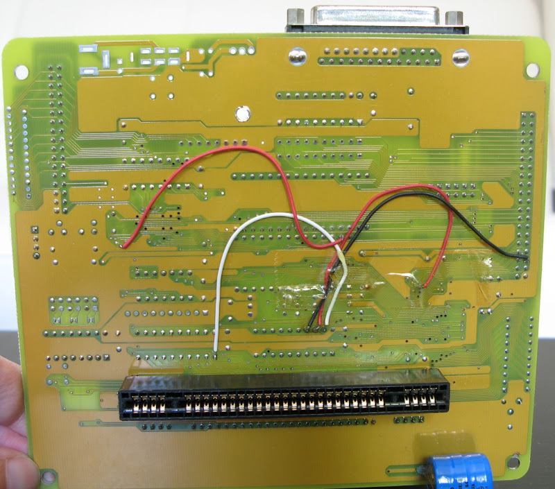
My unit also has the Motorola chip. However, it is possible to do the modification based on your photographs in my opinion. There are those three pins of the programmable logic chip that have been bent out of the socket. One of the wires connected to those pins goes to pin 1 of the 74LS245 bus buffer chip. When one checks where the other two wires go to on the bottom of the board, one sees that both are involved with the same pin of the memory board header. Instead of cutting a trace and soldering a wire into the middle of the board, I would cut the corresponding pin on the memory board itself as short as possible so that it no longer makes an electrical contact with the memory board connector of the main board. The wire which in the photograph is next to the cut trace would instead be soldered onto the same connector pin position on the memory board. The wire that in in the photograph is in a difficult to solder hole would instead be soldered in the place of the other wire, with the trace left intact.
Unfortunately it turns out that my soldering equipment and skills are not good enough for installing the additional memory chips onto the memory board. One alternative idea that I had would be to make an adapter board which takes 30-pin SIMMs and plugs into the memory board slot. That would be too high to fit into the SWC case though.
If you make the modification, please report your results.
|
|
| Back to top |
|
|
rcade
Joined: 13 Mar 2008
Posts: 30
|
| Posted: Sun May 11, 2008 1:32 am Post subject: |
|
|
I'll try it next week. My SWC has one of the PEELs soldered in, so I'll need to socket it to fit both chips in and didn't have any 20-pin DIPs on hand.
Ordered and on the way. If it works, I have 4 spare sets of PEELs if someone else wants to mod their own. I'd sell them for the price of blanks.
I got the RAM soldered on some time ago. It's not the prettiest job, but I think it's sound. We'll see if it'll pass the RAM test. 
|
|
| Back to top |
|
|
1541
Joined: 09 Apr 2008
Posts: 15
|
| Posted: Fri May 30, 2008 7:52 pm Post subject: |
|
|
With a fine soldering tip and some more practicing I finished the modification successfully. All 32 megabits are now recognized and games of this size load and play fine. Thank you for the instructions everyone. Here is a table of reverse-engineered connections on the memory board, it is useful for checking the soldering work. The format of the lines is as follows:
- header pin number
- chip identifier (or "all" for all memory ICs)
- pin number
- pin name
When the memory board has all eight chips installed, there can be two, four or eight memory chips connected to a same signal line. Sorry about the formatting, the forum software eats whitespace characters. The memory chip pin numbers are so-called JEDEC pin numbers (pins 6,7,8 and 19,20,21 do not exist).
1 U1,25,I/O4 U3,25,I/O4
2 U1,24,I/O3 U3,24,I/O3
3 U1,2,I/O2 U3,2,I/O2
4 U1,1,I/O1 U3,1,I/O1
5 U5,25,I/O4 U7,25,I/O4
6 U5,1,I/O1 U7,1,I/O1
7 U5,24,I/O3 U7,24,I/O3
8 U5,2,I/O2 U7,2,I/O2
9 U1,23,/CAS U2,23,/CAS U3,23,/CAS U4,23,/CAS
10 U5,23,/CAS U6,23,/CAS U7,23,/CAS U8,23,/CAS
11 U1,4,/RAS U2,4,/RAS U3,4,/RAS U4,4,/RAS
12 U5,4,/RAS U6,4,/RAS U7,4,/RAS U8,4,/RAS
13 all,18,A8
14 all,5,A9
15 all,17,A7
16 all,9,A0
17 all,16,A6
18 all,10,A1
19 all,15,A5
20 all,11,A2
21 all,14,A4
22 all,12,A3
23 U2,25,I/O4 U4,25,I/O4
24 U2,24,I/O3 U4,24,I/O3
25 U2,2,I/O2 U4,2,I/O2
26 U2,1,I/O1 U4,1,I/O1
27 U6,25,I/O4 U8,25,I/O4
28 U6,1,I/O1 U8,1,I/O1
29 U6,24,I/O3 U8,24,I/O3
30 U6,2,I/O2 U8,2,I/O2
31 U5,3,/WE U6,3,/WE
32 U7,3,/WE U8,3,/WE
33 U1,3,/WE U2,3,/WE
34 U3,3,/WE U4,3,/WE
35 U5,22,/OE U6,22,/OE
36 U7,22,/OE U8,22,/OE (this signal needs the modification discussed earlier in this thread)
37 U1,22,/OE U2,22,/OE
38 U3,22,/OE U4,22,/OE
39 all,10,VCC (+5V)
40 all,26,VSS (GND)
|
|
| Back to top |
|
|
Mystic_Merlin
Joined: 15 Oct 2007
Posts: 508
Location: Bangkok
|
| Posted: Sun Sep 19, 2010 5:06 pm Post subject: |
|
|
I recently got a 32M 2.8CC with that mod on a Goldstar version so here I took a few pics.
Goldstar TOP PCB
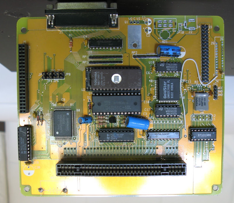
Download full size
Goldstar BOTTOM PCB
Download full size
To compare, here's a pic of a Motorola 24M 2.6CC
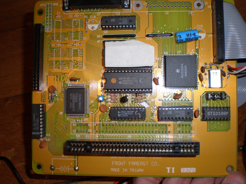
Thing is the Schweino's archive attached here is for the Motorola's 2 PEELs version, whereas the Goldstar version only uses one.
U12:
| Code: | JEDEC PEEL file Translated from: EP320 Thu 6-9-1994 16:10:45
SFC-C1X.JED
Target PEEL device = 18CV8
*QP20
*QF2696
*F0
*
N Output Pin 19*
L0000 1001 1111 1111 1111 1111 1111 1111 1111 1111 *
L0144 0111 1111 1111 1111 1111 1111 1111 1111 0111 *
N Output Pin 18*
L0288 1011 1111 1111 1111 1111 1111 1111 1111 0111 *
L0432 0111 1111 1111 1111 1111 1111 1111 0111 1111 *
N Output Pin 17*
L0576 1011 1111 1111 1111 1111 1111 1111 0111 1111 *
L0720 0111 1111 1111 1111 1111 1111 0111 1111 1111 *
N Output Pin 16*
L0864 1011 1111 1111 1111 1111 1111 0111 1111 1111 *
L1008 0111 1111 1111 1111 1111 0111 1111 1111 1111 *
N Output Pin 15*
L1152 1011 1111 1111 1111 1111 0111 1111 1111 1111 *
L1296 0111 1111 1111 1111 0111 1111 1111 1111 1111 *
N Output Pin 14*
L1440 1011 1111 1111 1111 0111 1111 1111 1111 1111 *
L1584 0111 1111 1111 0111 1111 1111 1111 1111 1111 *
N Output Pin 13*
L1728 1011 1111 1111 0111 1111 1111 1111 1111 1111 *
L1872 0111 1111 0111 1111 1111 1111 1111 1111 1111 *
N Output Pin 12*
L2016 1111 1011 1111 1111 1111 1111 1111 1111 1111 *
N Output Enable 19,18,...12*
L2304 1111 1111 1111 1111 1111 1111 1111 1111 1111 *
L2340 1111 1111 1111 1111 1111 1111 1111 1111 1111 *
L2376 1111 1111 1111 1111 1111 1111 1111 1111 1111 *
L2412 1111 1111 1111 1111 1111 1111 1111 1111 1111 *
L2448 1111 1111 1111 1111 1111 1111 1111 1111 1111 *
L2484 1111 1111 1111 1111 1111 1111 1111 1111 1111 *
L2520 1111 1111 1111 1111 1111 1111 1111 1111 1111 *
L2556 1111 1111 1111 1111 1111 1111 1111 1111 1111 *
N Sync Preset, Async Clear, Macrocell 19,18,...12*
L2592 0000 0000 0000 0000 0000 0000 0000 0000 0000 *
L2628 0000 0000 0000 0000 0000 0000 0000 0000 0000 *
L2664 0011 0011 0011 0011 0011 0011 0011 0011 *
C6311* |
U13:
| Code: | JEDEC PEEL file Translated from: EP320 Sat 5-21-1994 9:40:22
SFC-C22.JED
Target PEEL device = 18CV8
*QP20
*QF2696
*F0
*
N Output Pin 17*
L0576 1111 1111 1110 1111 1111 1111 1111 1111 1111 *
L0720 0111 1110 1111 1111 1111 1111 1111 1111 1110 *
N Output Pin 16*
L0864 1001 1111 1111 1111 1111 1111 1111 1111 1111 *
L1008 0111 1111 1111 1111 1111 0111 1111 1111 1111 *
N Output Pin 15*
L1152 1011 1111 1111 1111 1111 1111 1111 1111 0111 *
L1296 0111 1111 1111 1111 0111 1111 1111 1111 1111 *
N Output Pin 14*
L1440 1011 1111 1111 1111 1111 1111 1111 1111 1110 *
L1584 0111 0111 0111 0111 1111 1111 0111 1011 1111 *
N Output Pin 13*
L1728 1111 1011 1111 1111 1111 1111 1111 1111 1111 *
L1872 1111 1111 0111 0111 1111 1111 1111 1011 1111 *
N Output Enable 19,18,...12*
L2304 0000 0000 0000 0000 0000 0000 0000 0000 0000 *
L2340 0000 0000 0000 0000 0000 0000 0000 0000 0000 *
L2376 1111 1111 1111 1111 1111 1111 1111 1111 1111 *
L2412 1111 1111 1111 1111 1111 1111 1111 1111 1111 *
L2448 1111 1111 1111 1111 1111 1111 1111 1111 1111 *
L2484 1111 1111 1111 1111 1111 1111 1111 1111 1111 *
L2520 1111 1111 1111 1111 1111 1111 1111 1111 1111 *
L2556 0000 0000 0000 0000 0000 0000 0000 0000 0000 *
N Sync Preset, Async Clear, Macrocell 19,18,...12*
L2592 0000 0000 0000 0000 0000 0000 0000 0000 0000 *
L2628 0000 0000 0000 0000 0000 0000 0000 0000 0000 *
L2664 0011 0011 1011 0011 0011 1011 1011 0011 *
C405E* |
| Description: |
| 32M BIOS MOD for the SMS3201 |
|

Download |
| Filename: |
ATX-SW28.zip |
| Filesize: |
13.46 KB |
| Downloaded: |
1384 Time(s) |
|
|
| Back to top |
|
|
squale
Joined: 07 Mar 2013
Posts: 4
|
| Posted: Mon Mar 18, 2013 3:33 am Post subject: |
|
|
Hi,
I got exactly the same 2.6CC 24Mb Motorola as pictured, how can I upgrade it to 2.8CC/32Mb ?
Anyone could flash the chips ?
thx 
|
|
| Back to top |
|
|
cpsystem3
Joined: 07 May 2013
Posts: 24
|
| Posted: Wed May 22, 2013 3:08 pm Post subject: |
|
|
Resurrecting this thread as I'm about to embark on the ram upgrade modification myself...
I have a NTSC 24m unit, I believe Motorola processor (not goldstar).
I noticed the Motorola motherboard has solder lands for 4 additional memory IC's (U1 through U4 located in the upper right corner).
Has anybody tried installing ram chips in these locations? In theory, if the PEELs can properly map the memory, we can access 48m on this unit.
Thanks for any feedback..
|
|
| Back to top |
|
|
Mystic_Merlin
Joined: 15 Oct 2007
Posts: 508
Location: Bangkok
|
| Posted: Fri May 24, 2013 6:50 am Post subject: |
|
|
I seriously doubt the SWC can access 48M without adding some custom logic.
Those empty memory slots are a legacy from the Super Magicom. The Goldstar is actually the lastest revision, closer to the SWC DX.
To correct a previous post, the Goldstar also uses 2 PEELS, they're just labeled differently
|
|
| Back to top |
|
|
cpsystem3
Joined: 07 May 2013
Posts: 24
|
| Posted: Fri May 24, 2013 2:10 pm Post subject: |
|
|
| Mystic_Merlin wrote: | I seriously doubt the SWC can access 48M without adding some custom logic.
Those empty memory slots are a legacy from the Super Magicom. The Goldstar is actually the lastest revision, closer to the SWC DX.
To correct a previous post, the Goldstar also uses 2 PEELS, they're just labeled differently |
Without a doing a deep analysis on the PCB, the traces appear to be wired in series to the RAM board's input connector. I need to confirm with my multimeter, but I believe all lines are tied in.
Surely the PEEL's for the 32mbit upgrade won't suffice, but I am thinking its possible to figure out exactly what is changed in the PEEL source and hardware modifications for the 24m to 32m upgrade. If I can isolate the differences, I can probably extend the logic.
Has anyone dumped the 24mbit PEEL chips? Is the security bit blown? When I perform the 32mbit upgrade on mine, I'll attempt to dump the stock ones (and hopefully post) for archival & repair purposes.
On the other hand... maybe I should just be happy with 32mbit and purchase a larger capacity unit
|
|
| Back to top |
|
|
Mystic_Merlin
Joined: 15 Oct 2007
Posts: 508
Location: Bangkok
|
| Posted: Fri May 24, 2013 6:14 pm Post subject: |
|
|
| cpsystem3 wrote: |
Without a doing a deep analysis on the PCB, the traces appear to be wired in series to the RAM board's input connector. I need to confirm with my multimeter, but I believe all lines are tied in.
Surely the PEEL's for the 32mbit upgrade won't suffice, but I am thinking its possible to figure out exactly what is changed in the PEEL source and hardware modifications for the 24m to 32m upgrade. If I can isolate the differences, I can probably extend the logic.
Has anyone dumped the 24mbit PEEL chips? Is the security bit blown? When I perform the 32mbit upgrade on mine, I'll attempt to dump the stock ones (and hopefully post) for archival & repair purposes.
On the other hand... maybe I should just be happy with 32mbit and purchase a larger capacity unit |
Interesting indeed if you're up for the challenge 
I believe I have read in the past that some those PEELs are protected some are not, I'll guess you may figure it out pretty soon.
Although a very reliable machine, if there's one thing to be reworked first on that model, it's its GUI! It's even slower than a Pro Fighter.
|
|
| Back to top |
|
|
cpsystem3
Joined: 07 May 2013
Posts: 24
|
| Posted: Tue May 28, 2013 2:55 pm Post subject: |
|
|
Unfortunately my Xeltek 580u programmer is having trouble reading/writing the PEEL chips (which is odd because I program GAL's all the time).
That said, I was unable to dump the 24m stock PEEL chips. I will contact some guys I know who can read registered PAL chips, and look to send them out for dumping.
In the meantime, I have ordered some GAL18v10's to use. Attached are the converted PALTOGAL pre-converted JED source files for use on GAL18v10 chips. These are not tested as of yet, but I don't see any reason they will not work. In my past experience, PALTOGAL is very reliable.
| Description: |
| 32mbit PEEL18CV8 converted to GAL18v10L for Super Wild Card |
|
Download |
| Filename: |
SWC_32m_GAL18V10L.zip |
| Filesize: |
1.94 KB |
| Downloaded: |
1004 Time(s) |
|
|
| Back to top |
|
|
rcade
Joined: 13 Mar 2008
Posts: 30
|
| Posted: Wed Jun 12, 2013 1:05 am Post subject: |
|
|
| I've still got several sets of the programmed 32M PEELs if someone wants to make an offer.
|
|
| Back to top |
|
|
th3shep2007
Joined: 09 Jul 2016
Posts: 4
|
| Posted: Sat Jul 09, 2016 1:53 pm Post subject: |
|
|
Thread resurrection!!
Hi im looking to upgrade my swc sms3201 to 32mbit
I found some HM514400BLTT7 ram chips on ebay and have successfully soldered 2 onto the ram board.
Looking at the rest of your comments i need to replace some logic chips?
I have a blank AM27C128 EPROM ready to have the bios programmed to it but havent managed to do that yet.
Also mine is the board with the Motorola chips.
Any help would be greatly appreciated
|
|
| Back to top |
|
|
|
|
You cannot post new topics in this forum
You cannot reply to topics in this forum
You cannot edit your posts in this forum
You cannot delete your posts in this forum
You cannot vote in polls in this forum
You can attach files in this forum
You can download files in this forum
|
Powered by phpBB © 2001, 2005 phpBB Group
|

